In the previous posts (Part One, Part Two, Part Three) of this series, we examined the control to output transfer function or modulator of the three main power supply topologies. In the frequency domain, these topologies consist of a DC gain that is flat out to the resonance of an LC low pass filter. They will often contribute very little gain or bandwidth to feedback loop gain. In this blog post, we will examine the error amplifier or compensator, the ideal response of the loop gain, and the Type 1 amplifier or integrator.
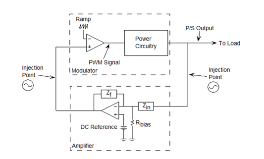
Figure 1.
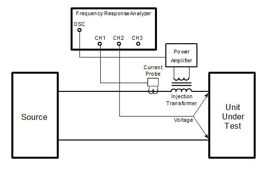
In Figure 1, the inverting input of the error amplifier, usually a voltage or transconductance op amp, senses the output voltage through a voltage divider and compares it to a reference voltage or set point on the positive input and the difference between them is output as an error signal. As frequency increases, the open loop gain of the op amp drops. Also, reactive components and time delays will cause phase shifts. If the phase shift, including the op amp inversion, reaches 360 degrees and the gain is greater than 1, the loop will oscillate since the feedback is now positive. To avoid this problem, the feedback loop of the error amplifier is designed by taking into account the response of the power stage of the power supply. It is then measured to ensure the compensation will provide enough gain, bandwidth, phase margin for the switching power supply to meet specifications.
What are the ideal characteristics of the overall loop gain in a switch mode power supply feedback loop? The gain must be large at DC in order to minimize steady state error. The bandwidth should be as high as possible to provide fast response to line and load changes. The gain should cross the 0 dB gain with a slope of -1 or -20 dB/decade to have an adequate phase margin. The phase margin should be set so that there is adequate rise time but minimal overshoot and settling time. In the expression for the loop gain, -GH, going around the loop, the error amplifier, H, is in series with the power stage, G, so it can be used to control the loop gain response since the error amplifier op amp has the excess gain and bandwidth to do so.
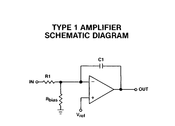 Figure 2
Ideally, the overall loop gain should resemble an inverting integrator and the error amplifier will be used to obtain this response as closely as possible. As a first iteration, we can use an op amp integrator as an error amplifier. The type 1 amplifier or integrator has a single pole roll off which is shown in Figure 2. The gain of this amplifier is the open loop gain at low frequencies. The gain ideally rolls off forever with a slope of -1 and the phase shift is fixed at -270 degrees as plotted in Figure 3.
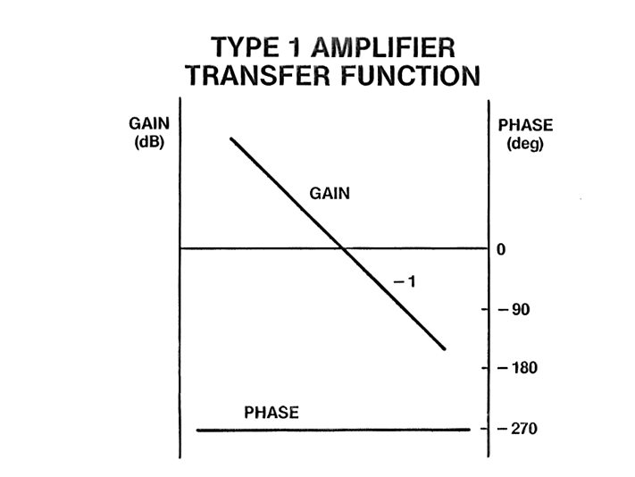
Figure 3
The gain of the Type 1 amplifier is given in Equation 1. The 0 dB crossover frequency can be found by setting the gain to 1. To start a design, R1 can be any arbitrary value chosen by the user. A good starting point is 10 k ohms. The size of this resistor will influence the size of the capacitor in the error amp feedback. The objective of the error amplifier design is to have the loop gain crossover at 0 dB gain with a -1 slope. The type 1 amplifier can only be used to crossover where the modulator gain is flat or has 0 slope since it has a constant -1 slope. This point will have to be below the LC corner frequency where there is little phase shift. At the crossover point, there is 180 degrees of phase shift around the loop from the amplifier inversion and the -1 slope will add an extra 90 degrees of phase so there will be about 90 degrees of phase margin, more or less. The gain of the type 1 compensator is set to the inverse of the modulator gain at the crossover frequency and with the gain, frequency, and the resistance R1 known, the value for C1 Is calculated.

Equation 1 shows that the resistor Rbias has no effect on the gain as shown in Figure 2. That is because it is connected between an ac virtual ground and ground. Rbias is used to set the power supply DC operating point. The Rbias value can be calculated using Equation 2 where the voltage reference, Vref, and the common mode voltage, Vcm, are equal when Vref is connected directly to the non-inverting op amp input. Vin is the output voltage of the power supply and R1 is the input resistor of the voltage divider.

The Type 1 amplifier does improve the steady state error but the transient response is poor due to the low crossover frequency. The gain response with a fixed -1 slope and the fixed phase shift of the amplifier limits the crossover frequency to the flat portion of the modulator response below the LC corner.
In the next blog post, we will examine the Type 2 and Type 3 amplifiers which will allow the loop to be crossed over at a specific frequency and phase margin above the modulator LC corner frequency using the K factor.
Related Content Posts
New Signal Injection Technique Simplifies Power Supply Feedback Loop Measurement
When to Use a Bode Box Injection/Isolation Transformer
Feedback Loop Injection Levels for Measuring Loop Gain
Best of Content - Loop Stability Analysis